
Summary
Most Doppler speed detectors offload signal processing to software: sample the received signal digitally, run an FFT, extract the frequency peak in firmware. This project does none of that. Every function that software would ordinarily handle, including amplification, bandpass filtering, frequency mixing, zero-crossing detection, and frequency-to-voltage conversion, is implemented as a dedicated hardware stage, designed and debugged from first principles. The Arduino Nano does exactly one thing: generate a stable 40 kHz carrier via hardware PWM.
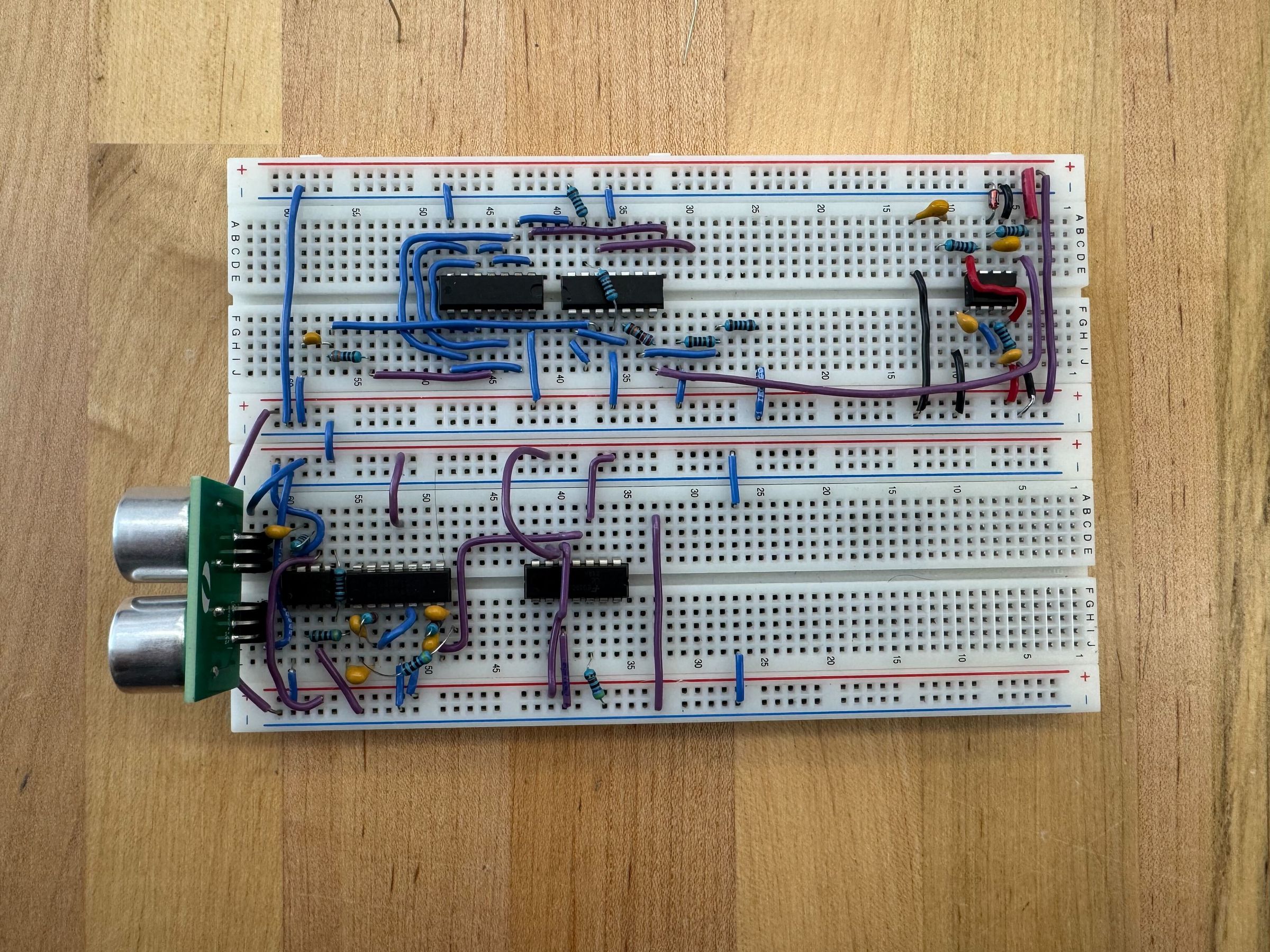
Built as a first-year student during the Spring 2026 Introduction to Sensing, Instrumentation and Measurement (ISIM) course at Olin College of Engineering, the result is an 11-stage discrete analog signal chain that converts the Doppler shift from a moving hand or walking person into a DC voltage on a voltmeter in real time. The path to a working circuit included a failed attempt at a hand-wound double-balanced mixer that had to be diagnosed, understood, and replaced before the system came to life.
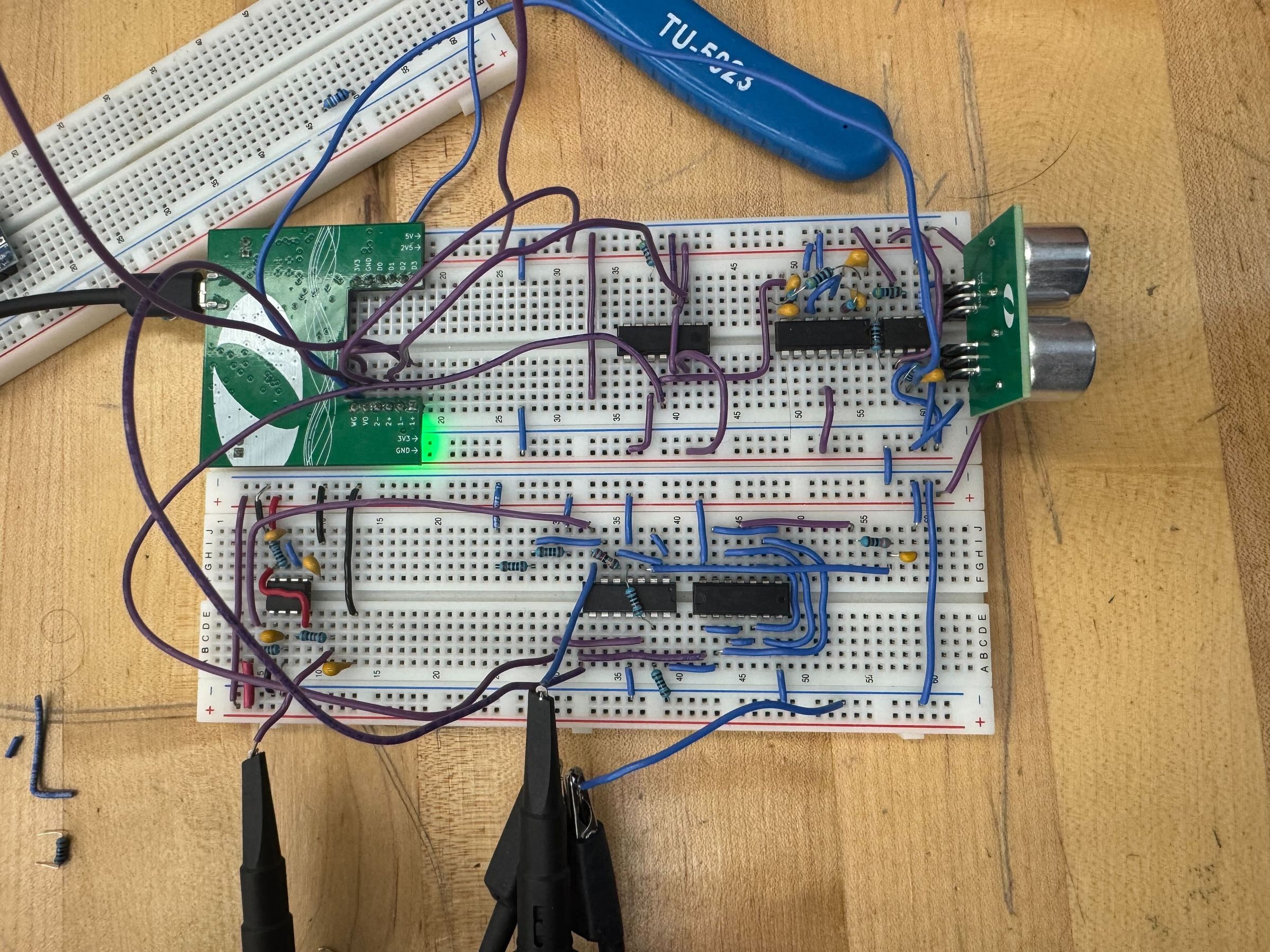
How It Works
When a sound wave reflects off a moving object, the reflected frequency shifts relative to the transmitted frequency. This shift, called the Doppler shift, is proportional to the object's radial velocity:
f_D = 2 · v · f₀ / cWhere f_D is the Doppler shift (Hz), v is object speed (m/s), f₀ is the carrier frequency (40,000 Hz), and c is the speed of sound (343 m/s). At 40 kHz, an object moving at 1 m/s produces a Doppler shift of approximately 233 Hz, well within the audible range and measurable with simple analog circuitry. Extracting and converting that low-frequency shift to a DC voltage is the core engineering problem this circuit solves.
Signal Chain
The circuit implements 11 discrete stages in sequence. Each stage was validated independently on an oscilloscope before integration.
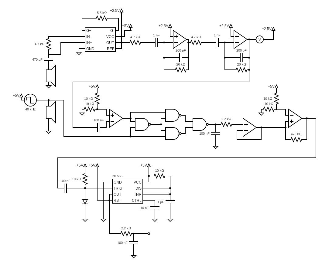
Stage 1: Carrier Generation (Arduino Nano, Timer2 PWM)
The Arduino Nano generates the 40 kHz transmit signal on pin D3 using Timer2 in Phase Correct PWM mode. This was a critical implementation detail: Fast PWM on Timer2 produced 80 kHz because it uses single-slope counting (0 to TOP only). Phase Correct PWM uses dual-slope counting, which halves the effective output frequency to exactly 40,000 Hz.
TCCR2A = COM2B1 | WGM20
TCCR2B = WGM22 | CS20
OCR2A  = 199
Result: 16 MHz / (2 × 200) = 40,000 Hz
This signal drives the TX transducer and simultaneously serves as the reference input to the mixer.
Stages 2 and 3: Ultrasonic Transduction and Instrumentation Amplifier
HC-SR04 ultrasonic elements serve as discrete TX and RX transducers operating at their 40 kHz resonance. The received signal is a small, noisy AC waveform riding on top of common-mode interference from the environment.
The first active stage is an AD623 instrumentation amplifier configured at approximately 100x gain using a single gain-setting resistor. The AD623 was chosen for its high input impedance (avoiding transducer loading), differential input (rejecting common-mode noise), and single-supply compatibility. Its reference pin is biased at 2.5 V to center the amplified signal within the 0-5 V supply range.
A 4.7 kΩ pullup resistor to 5 V with a 100 nF AC coupling capacitor at the input node prevents the signal from sitting near 0 V and clipping on the input rail, which resolved a significant early debugging issue.
Stage 4: 40 kHz Active Bandpass Filter
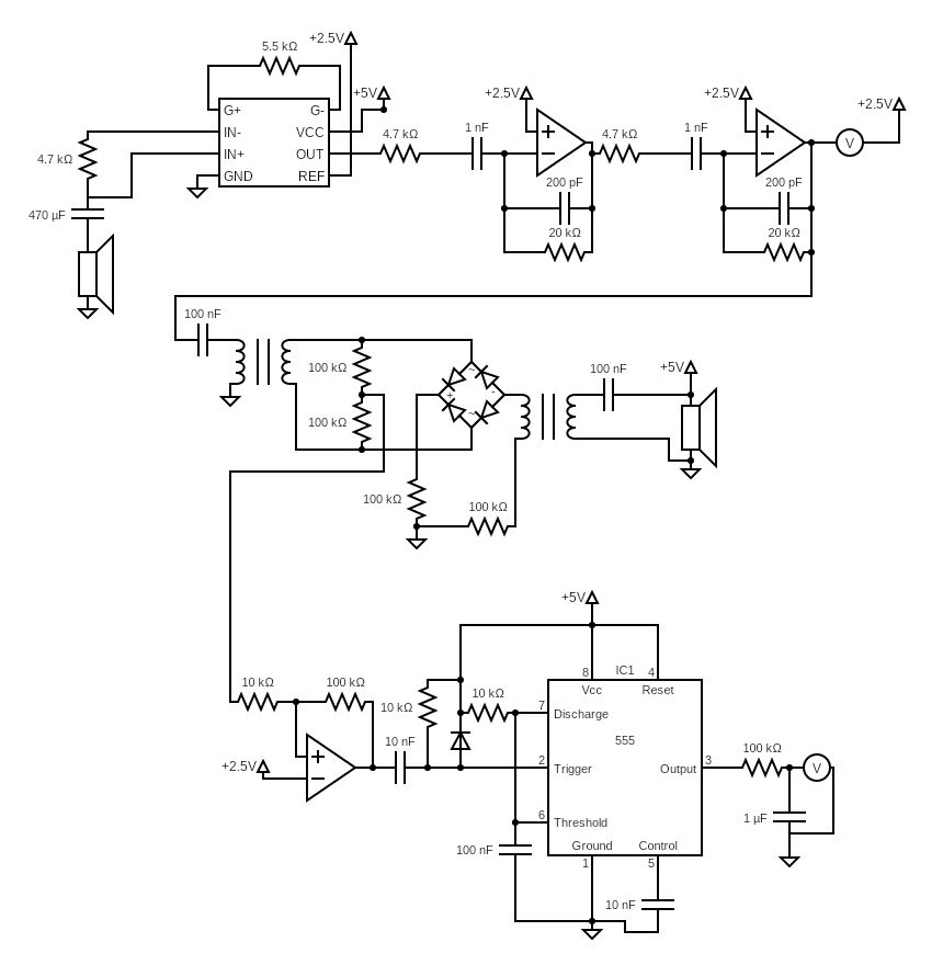
Two cascaded inverting op-amp stages (LMC6484) simultaneously amplify and filter the received signal. Each stage uses R1 = 4.7 kΩ and C1 = 1 nF for the lower cutoff (approx. 33.9 kHz), and R2 = 20 kΩ and C2 = 150 pF for the upper cutoff (approx. 53.1 kHz). This gives a passband of approximately 33.9 to 53.1 kHz centered on 40 kHz, with 4.26x gain per stage.
Distributing gain across multiple stages rather than a single high-gain block reduces the risk of instability and made it straightforward to verify each stage independently on the oscilloscope before proceeding.
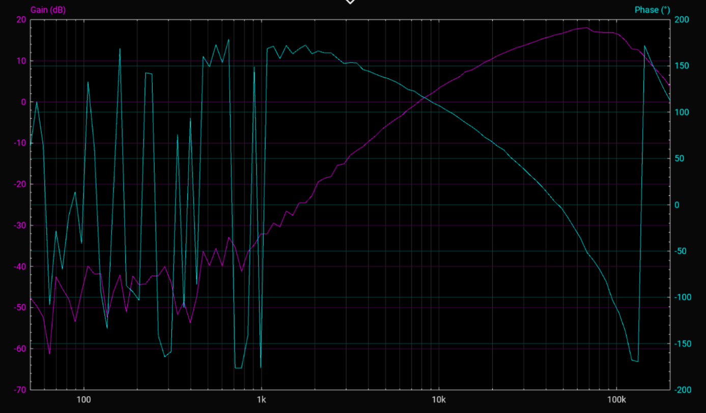
Stage 5: RX Comparator
An LMC6484 in open-loop comparator configuration converts the amplified analog receive signal into a 0-5 V square wave referenced to 2.5 V. This digitization step is what makes the XOR mixing approach in the next stage viable.
Stage 6: XOR Mixer (CD74HCT00E NAND Gates)
Frequency mixing is the heart of the Doppler extraction problem: to recover the shift between the transmitted and received frequencies, you need to multiply the two signals together. For analog signals, that requires transformers or analog multiplier ICs. Once both signals are at logic level, a gate does the same job.
That is the key insight that Stage 5 unlocks. Because the received 40 kHz has already been digitized into a square wave, XOR-ing it against the transmit reference produces sum (f_t + f_r) and difference (f_t - f_r) components directly. The difference component is the Doppler shift. A CD74HCT00E quad NAND gate IC wired as an XOR gate performs this on a single 5 V supply with no bias voltages, no transformers, and no negative rail.
The reason this was not the first approach, and why a hand-wound double-balanced mixer was attempted first, is covered in the Mixer Design section below.
Stage 7: Post-Mixer Low-Pass Filter
A first-order RC filter (2.2 kΩ + 100 nF, cutoff approx. 723 Hz) immediately after the XOR output rejects the 80 kHz sum component and 40 kHz carrier feedthrough, leaving only the Doppler signal in the range expected for hand and walking motion (tens to a few hundred Hz).
Stages 8 and 9: Buffer and Zero-Crossing Comparator
A unity-gain LMC6484 voltage follower isolates the RC filter output from the downstream comparator, preventing input impedance loading from shifting the filter's frequency response.
The zero-crossing comparator is where noise becomes a real problem. A naive implementation without hysteresis is unusable: a noisy Doppler signal hovering near the 2.5 V threshold fires multiple false edges per zero crossing, and the NE555 downstream would interpret each spurious edge as a real Doppler event. The result is phantom speed readings that bear no relation to actual motion. A 470 kΩ feedback resistor from output to non-inverting input creates approximately 5 mV of hysteresis, wide enough to reject typical noise but narrow enough to preserve timing accuracy at the lowest expected Doppler frequencies. The 2.5 V reference is set by a 1 kΩ / 1 kΩ voltage divider from the 5 V supply.
Stages 10 and 11: Frequency-to-Voltage Conversion and Peak Hold
The NE555 in monostable mode is the mechanism for frequency-to-voltage conversion: each rising edge from the Doppler square wave triggers a fixed-width 5 V output pulse. With 10 kΩ and 1 µF timing components, each pulse is exactly 11 ms wide. A 10 kΩ + 1 µF RC averaging filter integrates the pulse stream into a DC level. Because every pulse carries the same amplitude and duration, the average voltage is determined solely by how often pulses arrive, which is the Doppler frequency. Higher frequency means more pulses per second and a proportionally higher DC output. This is a hardware frequency-to-voltage converter with no software involvement.
A 100 nF differentiator capacitor and 1N914 diode extract the rising edges and clamp negative-going transients to protect the 555 trigger input. The timing capacitor was tuned from an initial 4.7 nF to 1 µF to widen the output pulse and increase voltage swing per pulse, improving sensitivity at the low end of the speed range.
The expected voltage-to-speed transfer function, derived from first principles:
V_out = V_p · τ · f_D = 5 V × 0.011 s × (2v × 40000 / 343) ≈ 1.17 · vWhere V_out is in volts and v is in m/s. A peak hold circuit (1N914 diode, hold capacitor, LMC6484 buffer, reset pushbutton) captures and holds the maximum speed reading for display on a voltmeter.
Mixer Design: From DBM to XOR
The mixer stage went through two iterations before reaching the final implementation.
Attempt 1: Double-Balanced Mixer with Hand-Wound Transformers
The first approach used a classic double-balanced mixer (DBM) topology with hand-wound FIT88-5 toroid transformers using bifilar and interleaved winding techniques, paired with 1N914 diodes. A DBM offers strong carrier suppression, which is desirable because the 40 kHz carrier at the mixer output would otherwise overwhelm the comparatively weak Doppler signal.
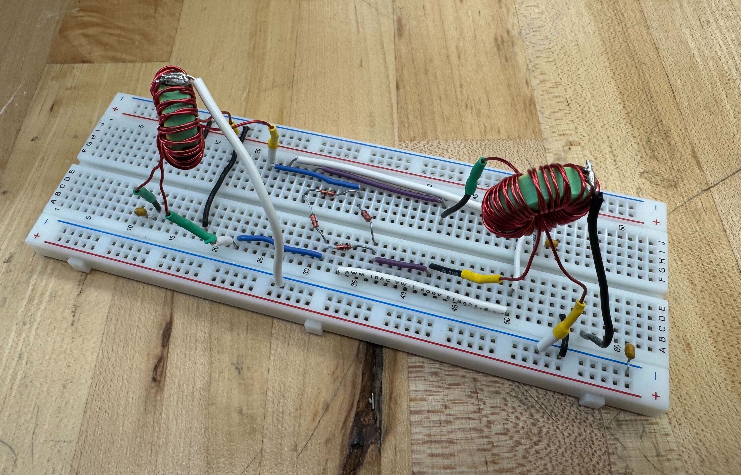
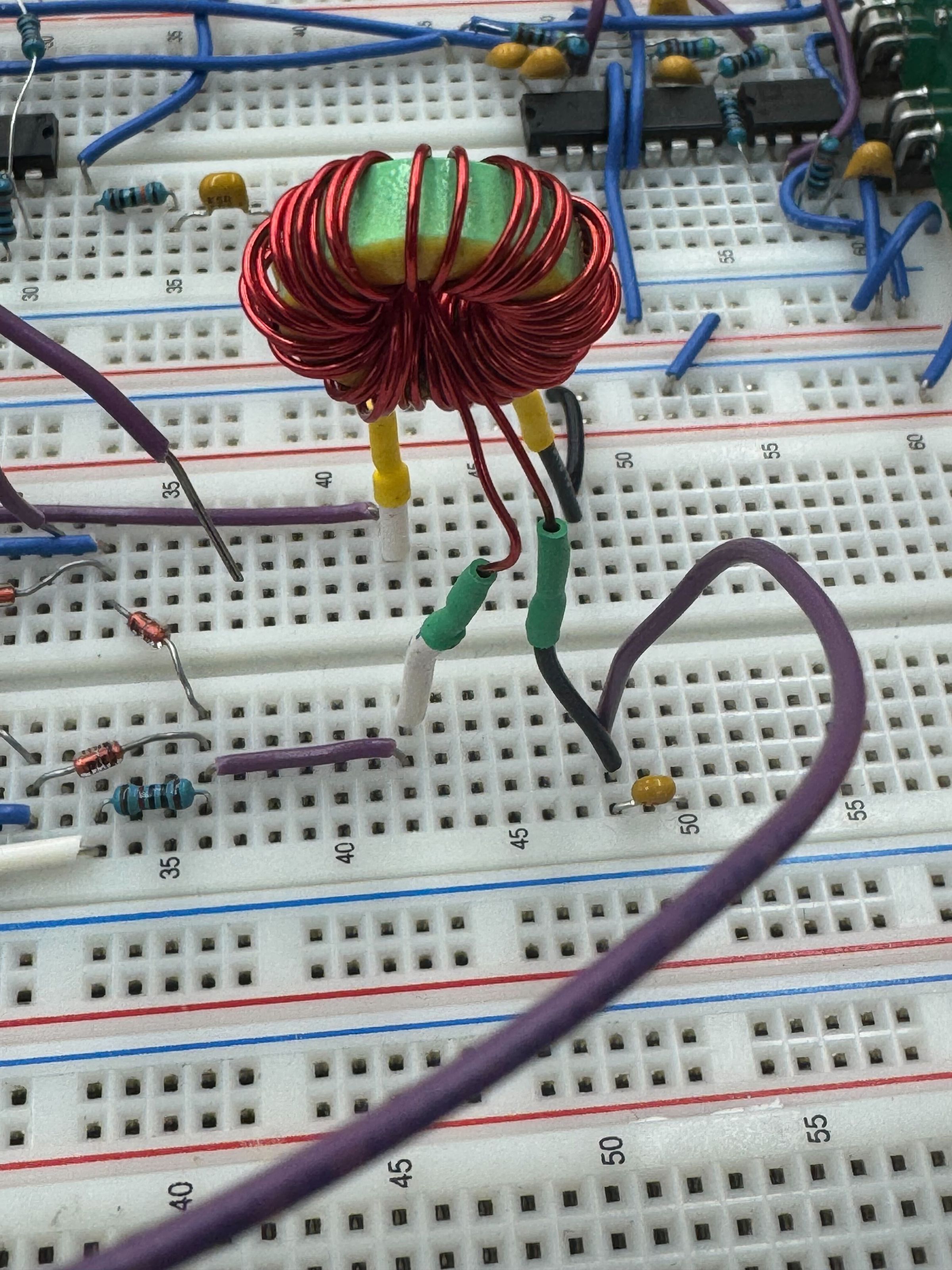
In practice, achieving adequate transformer balance with hand-wound toroids at these signal levels proved unreliable. Winding asymmetry caused carrier leakage and noise to dominate the mixer output, masking the Doppler signal entirely. Two winding configurations were attempted, including a physical center-tap approach, and neither produced usable results.
Final Implementation: XOR Switching Mixer (CD74HCT00E)
Replacing the DBM with an XOR gate built from NAND gates resolved both issues. Because both mixer inputs are already logic-level square waves at this point in the chain, no additional conversion is needed. The XOR output directly contains the sum and difference frequency components, and the downstream RC low-pass filter handles carrier rejection in place of transformer-based suppression. While square-wave mixing introduces harmonic content that a sine-wave DBM would avoid, it produced clean, repeatable Doppler output where the DBM had not, and required no components beyond the NAND gate IC already on hand.
Results
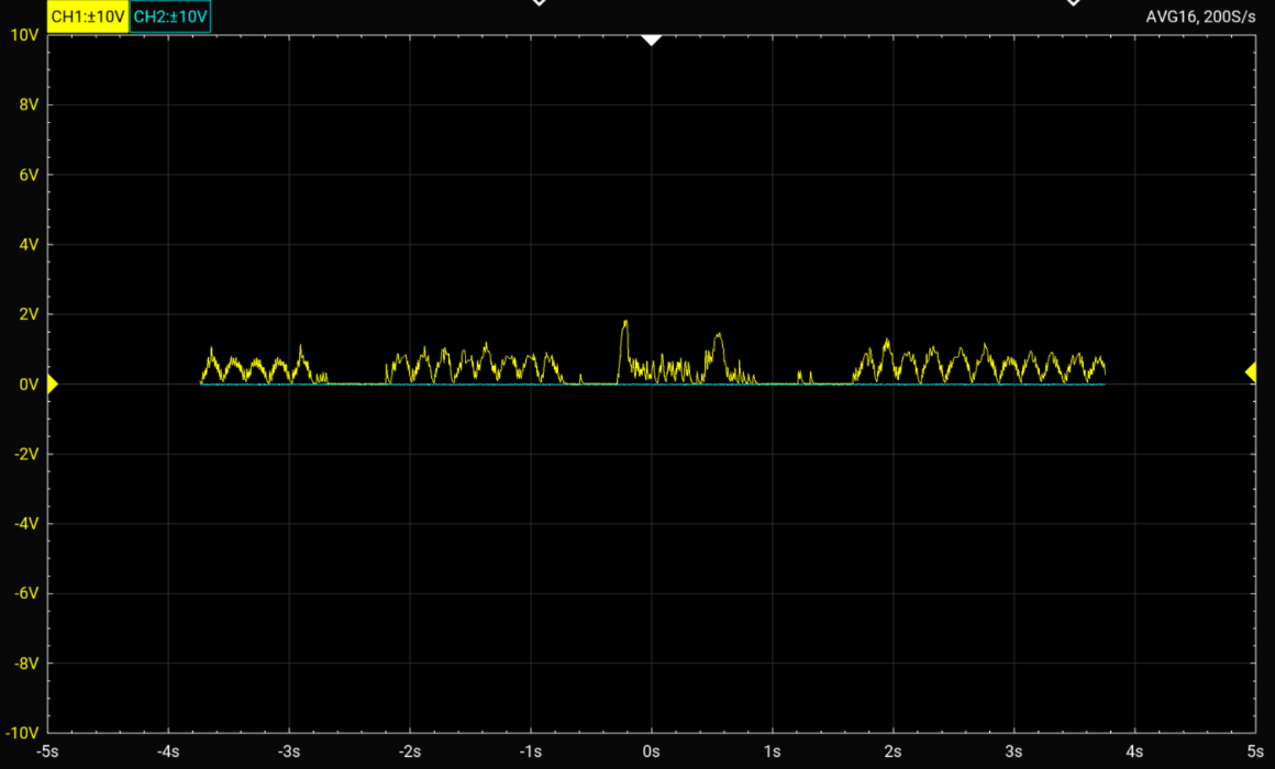
The completed circuit was tested by moving a hand toward and away from the transducers at varying speeds.
| Motion | Measured V_out | Estimated Speed |
|---|---|---|
| Stationary | ~0 V | 0 m/s |
| Normal hand shaking | 0.5 to 1.0 V | 0.43 to 0.85 m/s |
| Fast hand motion | 1.5 to 2.0 V | 1.3 to 1.7 m/s |
Output was oscillatory rather than constant, which is physically expected: hand velocity changes continuously in direction and magnitude during the test. The measured response corroborates the V_out = 1.17v transfer function derived from circuit parameters. Watching a voltmeter deflect in real time to hand speed, driven entirely by discrete analog circuitry with no software processing, is a concrete confirmation that the physics and the hardware are aligned across all 11 stages.
What This Project Demonstrates
This project is evidence of an ability to design a complete measurement system from a physical phenomenon down to a readable output, treating no layer as a black box. The debugging arc, spanning transformer winding imbalance, PWM frequency error, and input biasing fault, reflects systematic thinking that applies directly to more complex mixed-signal systems. It is the kind of work that shows what an engineer does when a textbook formula and a working circuit are still very far apart.