
Summary
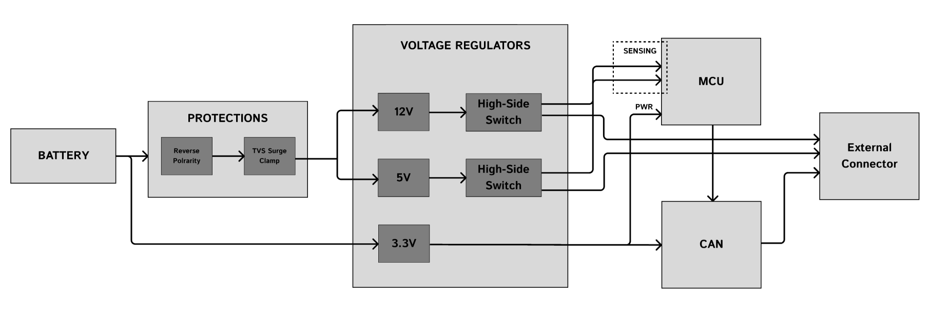
I designed a custom Power Distribution Board (PDB) for Olin Baja's off-road race vehicle, replacing ad hoc battery wiring with a centralized, protected power architecture. The board accepts a 9–12 V battery input and generates three regulated rails: 12 V, 5 V, and 3.3 V to power the vehicle's telemetry sensors, network supervisor, and auxiliary embedded subsystems. Total output capability is approximately 124 W across all rails, with reverse-polarity protection, TVS surge clamping, per-rail current limiting, and MCU-supervised rail control built in.
Motivation
Baja is transitioning to a data-driven development workflow, with increasing reliance on onboard telemetry and distributed sensing to tune vehicle performance. As the sensor suite expanded, two electrical needs became critical: reliable power distribution and low-noise, well-regulated voltage rails for sensitive electronics.
Previously, subsystems were powered directly from the 12 V battery bus. This was insufficient for mixed-voltage electronics. Several boards require regulated 5 V and 3.3 V supplies and are sensitive to supply variation and noise. The PDB was developed to centralize conversion and distribution so each subsystem receives the correct regulated rail from a single, documented power architecture.
Technical Highlights
Power Architecture
| Rail | Regulator Topology | Max Output | Key Loads |
|---|---|---|---|
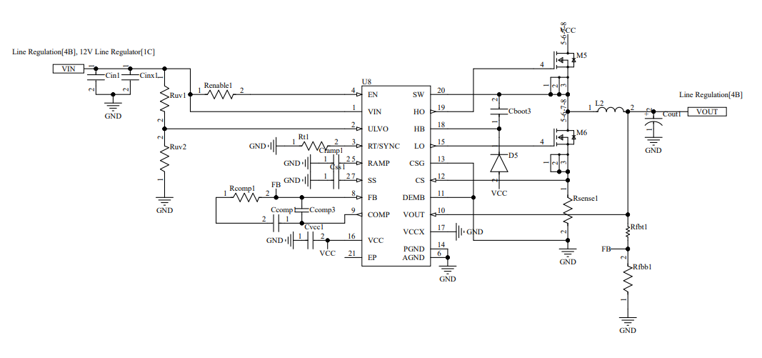
| 12 V | Synchronous 4-switch buck-boost (TI LM5176) | 6 A | High-current peripherals, sensor excitation |
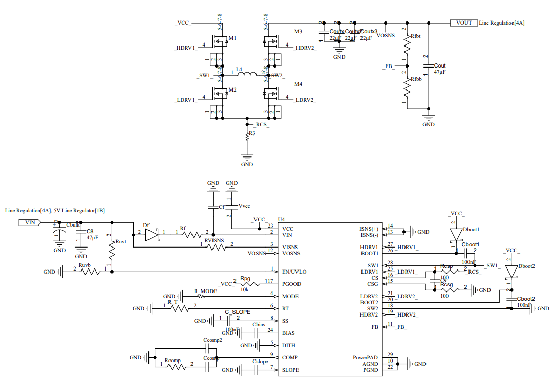
| 5 V | Synchronous buck (TI LM25116) | 10 A | Network supervisor board, sensors |
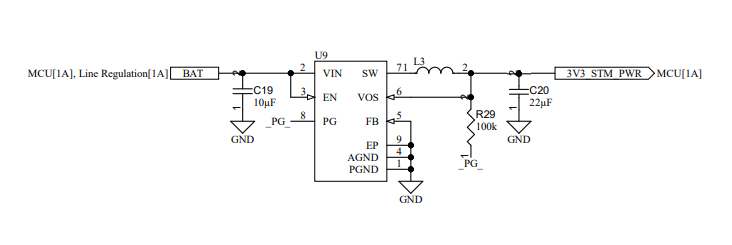
| 3.3 V | Step-down (TI TPS62162) | 0.5 A | STM32F405 MCU, status LEDs |
- Total output capability: ~124 W continuous
- Input range: 9–12 VDC
- Output voltage tolerance: ±5% on all rails at full load
- Operating temperature: -10°C to +50°C
Each rail is generated by a dedicated switching stage with its own inductor, output capacitance, and feedback network. The buck-boost topology on the 12 V rail maintains regulation even when the battery sags below 12 V under load.
Input Protection
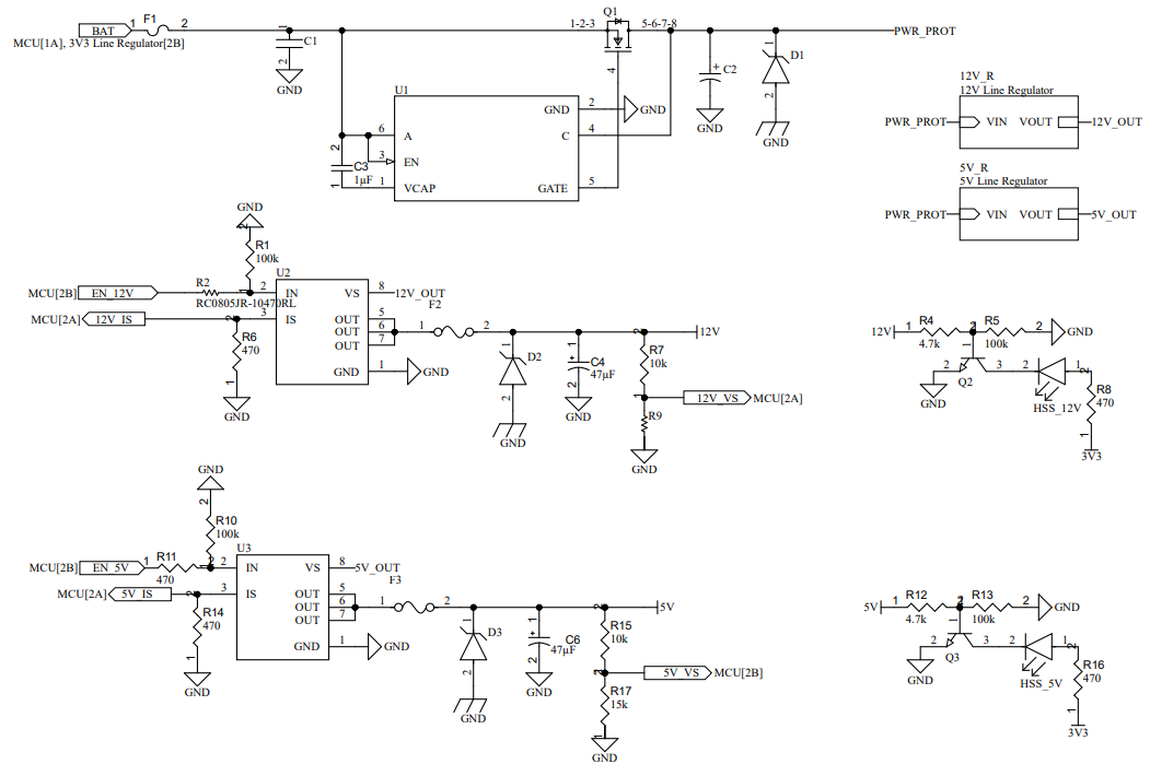
- Reverse-polarity MOSFET: Chosen over a series diode to minimize conduction losses at 6 A+ input current. A MOSFET's milliohm RDS(on) dissipates far less power than a Schottky diode's forward drop.
- 40 V TVS surge clamping: Absorbs transient spikes from hot-plug events and inductive loads on the vehicle harness.
- Rail-level protective elements at regulator outputs prevent upstream faults and transients from propagating into logic and sensor rails.
Distribution and Switching
- High-side switches (
HSS_12V,HSS_5V) provide MCU-controlled load distribution with overcurrent protection. - Per-rail fusing for additional fault-current limiting.
- Rail status LEDs and test points on all rails (
12V,5V,3V3,GND) for rapid bench bring-up and field debugging.
Control and Telemetry
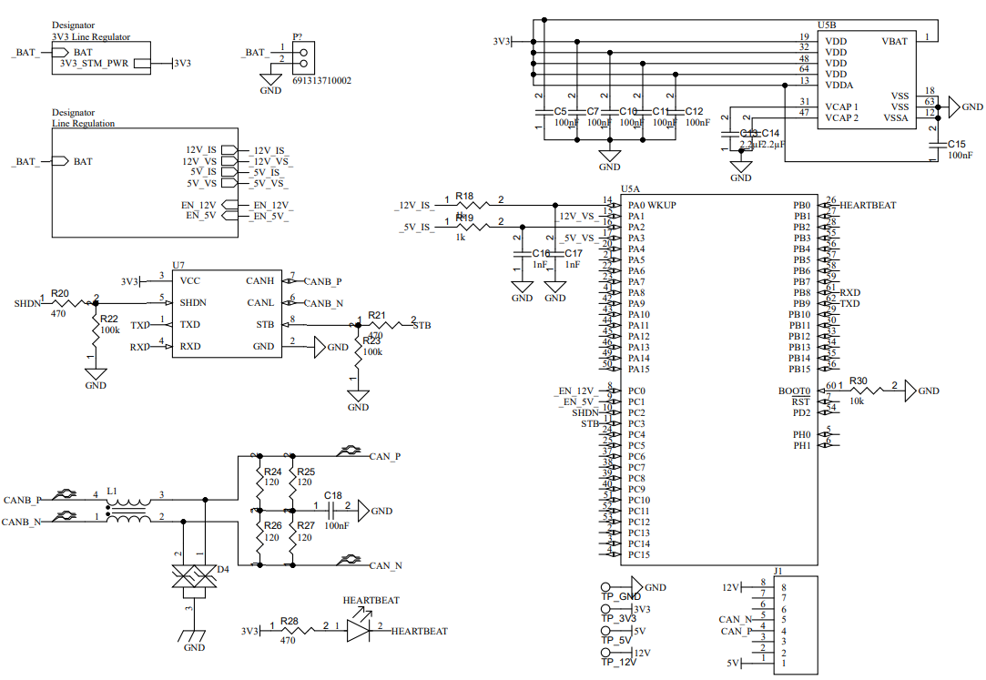
An on-board STM32F405 supervises rail behavior through:
- Enable lines (
EN_12V,EN_5V) for software-level startup sequencing - Current-sense feedback (
12V_IS,5V_IS) for load monitoring - Voltage-sense feedback (
12V_VS,5V_VS) for rail health verification - Heartbeat output for rapid "board alive" verification during bring-up
A CAN bus interface (transceiver with common-mode choke, termination, and ESD protection on CAN_P/CAN_N) transmits power telemetry to the CAN network for real-time monitoring and post-session analysis.
Mechanical
- Board size: 80 × 100 mm
- 2-layer stackup, optimized for small-batch fabrication cost.
Schematic and Layout
Schematic Organization
The schematic is partitioned by function so each block can be reviewed independently and debugged in isolation:
- MCU + CAN + I/O: Microcontroller, CAN transceiver, test points, and heartbeat indicator
- Line Regulation and Distribution: Battery input protection, rail enable/control, current/voltage sense, and high-side switch blocks
- 5V Regulator: Switching regulator, compensation network, and MOSFET/inductor/output filter
- 12V Regulator: High-power switching stage, dual gate-drive/power stage, and feedback/sense network
- 3.3V Regulator: Local buck stage for logic/MCU rail (
3V3_STM_PWR)
PCB Floorplan
The PCB is physically zoned by function: 12 V regulation, 5 V regulation, 3.3 V regulation, protection, MCU, CAN, and HSS distribution, to minimize interference between high-current switching loops and sensitive control/communication circuitry.
Layout priorities:
- Keep switching loops compact (MOSFET–driver–inductor–capacitor)
- Keep CAN protection and choke close to connector entry
- Maintain easy probe access to test points and key nets
Design Decisions & Trade-offs
| Decision | Rationale |
|---|---|
| MOSFET reverse-polarity protection | At 6 A+ input current, a MOSFET dissipates far less power than a Schottky diode's forward drop. |
| Separate switching stages per rail | Better regulation and domain isolation; prevents load transients on one rail from affecting others. |
| Separate 3.3 V regulator from 5 V bus | Isolates the MCU supply from load transients on the high-current 5 V bus, reducing the risk of brownouts or noise coupling into the digital domain. |
| Buck-boost for 12 V rail | The battery voltage can sag below 12 V under load; a buck-boost topology maintains regulation across the full 9–12 V input range. |
| MCU rail supervision | Enable lines and current/voltage feedback allow telemetry-driven diagnostics and software-controlled startup sequencing. |
| CAN for telemetry | Aligns with the existing vehicle network protocol, avoiding additional wiring or protocol bridges. |
| Test points + heartbeat + status LEDs | Faster bring-up and troubleshooting both on the bench and in the field. |
Schematics
Skills Demonstrated
- Power electronics design: Switching regulator selection, inductor/capacitor sizing, feedback loop compensation
- Circuit protection: TVS selection, MOSFET-based reverse polarity, high-side switch overcurrent limiting
- Embedded integration: STM32 ADC signal conditioning, CAN bus communication, software-controlled rail management
- PCB design: High-current 2-layer layout, functional zone partitioning, thermal management, design-for-test
- Systems thinking: Translating vehicle-level electrical needs into a documented, testable board-level architecture
Status & Next Steps
The board is currently in validation. Planned improvements for the next revision include:
- NTC thermistor for on-board temperature monitoring
- Battery state-of-charge estimation