
Summary
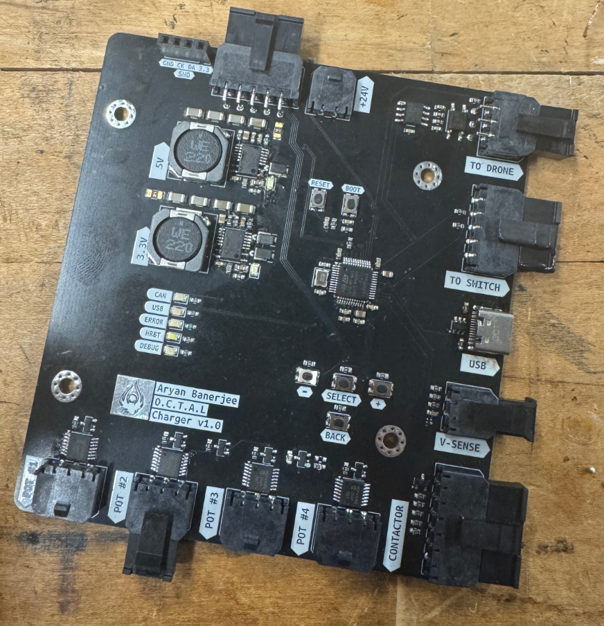
The O.C.T.A.L Charger v1.0 is a custom STM32-based controller PCB for a four-channel, ~24kW LiPo charging system built for the O.C.T.A.L heavy-lift drone. The board does not carry charging current. It controls four industrial open-frame power supplies (30–60V, ~120A each) by replacing each PSU's manual voltage-setting potentiometer with an MCP41U83 SPI digital potentiometer, giving firmware real-time control over PSU output voltage per channel. A high-power contactor on each channel, driven through an optoisolated path, gates the PSU output to the battery while providing current sensing. The STM32 senses battery voltage and current, exposes USB-C for bench configuration, and includes CAN-FD hardware for planned drone/BMS integration.
| Role | Solo hardware and firmware owner |
| Stack | KiCad 9, STM32G473, C, SPI, ADC, USB CDC, CAN-FD |
| Status | Fabricated and partially validated |
| Impact | Custom controller enabling four parallel LiPo charge channels with firmware-controlled PSU voltage, per-channel sensing, isolated switching, and planned CAN-FD integration |
I designed this controller end-to-end: schematic capture across a seven-sheet KiCad 9 hierarchy, PCB layout and Gerber handoff, STM32 firmware bring-up, and bench debugging on the first revision. Core subsystems are validated on the fabricated board.
Motivation
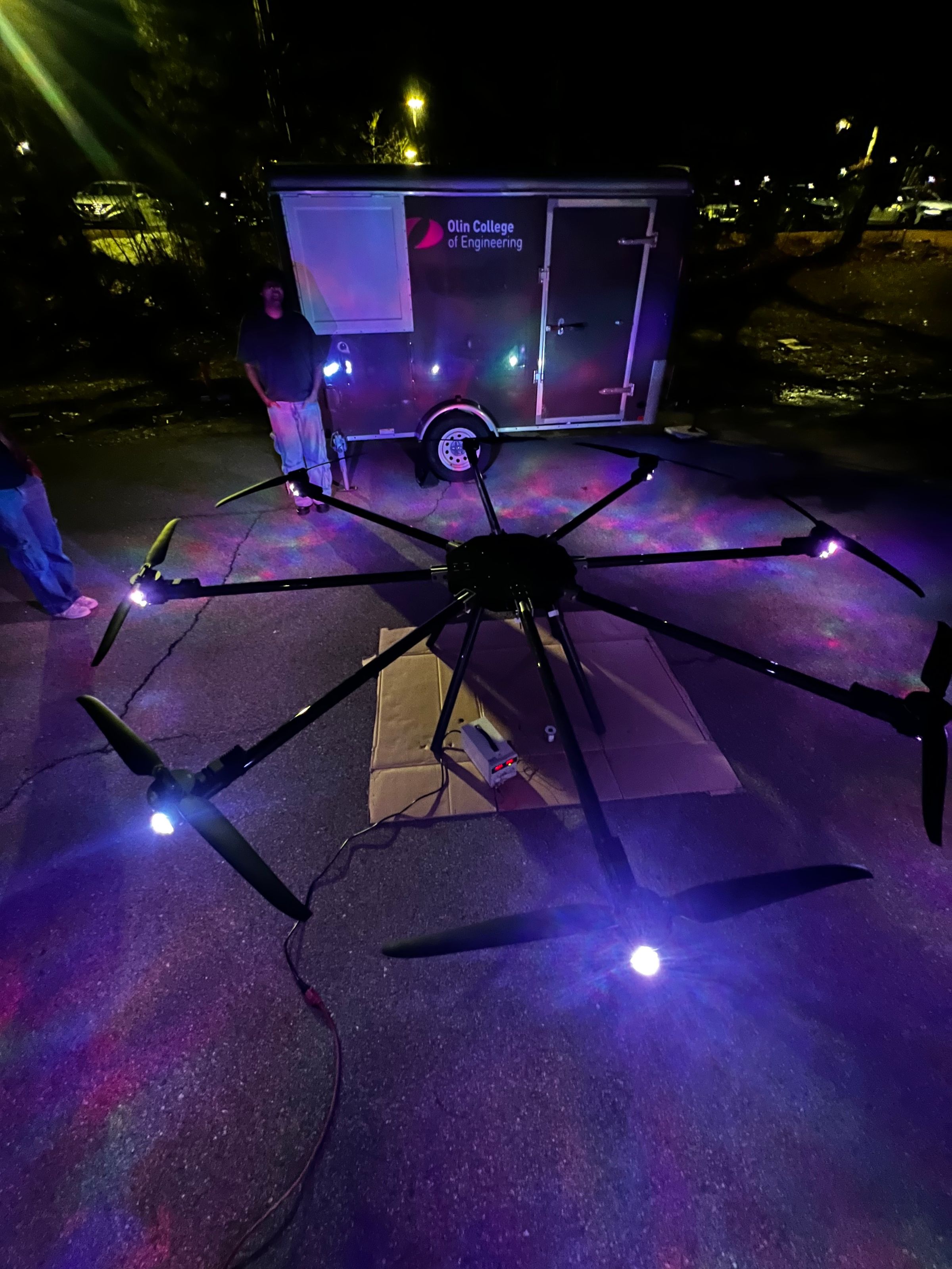
The O.C.T.A.L drone is powered by four custom-built high-capacity LiPo battery packs. Charging them simultaneously at the required power level (roughly 6kW per channel) rules out most commercial options: multi-channel chargers capable of this are very expensive, and none offer CAN-FD integration or the per-channel isolation the platform requires.
Industrial open-frame power supplies handle the heavy current; the O.C.T.A.L Charger board adds the intelligence: replacing each PSU's manual potentiometer with a digitally-controlled equivalent so firmware can manage charging across all four channels simultaneously and report status over the drone's CAN network.
System Architecture
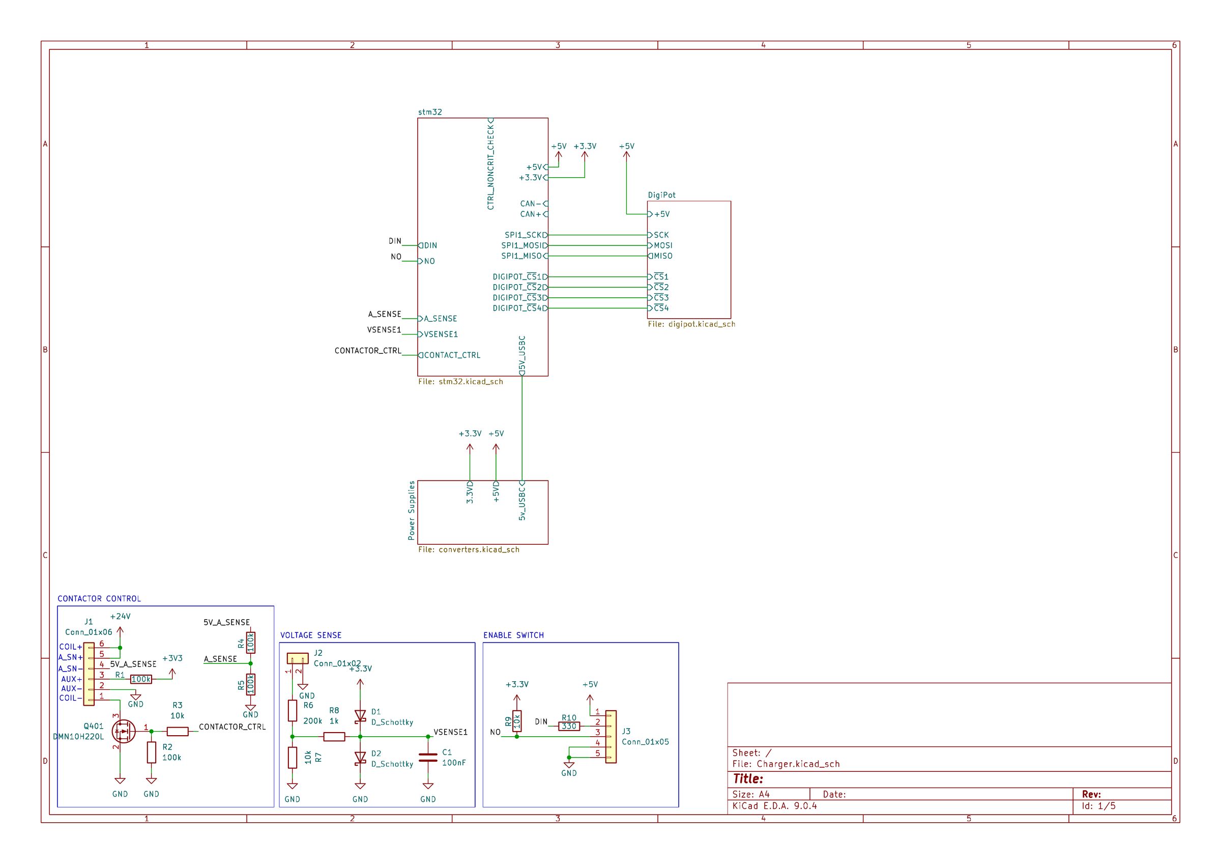
The design is organized across seven KiCad sheets: a top-level contactor and voltage-sense sheet, two DC-DC converter sheets, an STM32 and peripherals sheet, a DigiPot charge control sheet, and a USB-C interface sheet.
The 24V input steps down to 5V and 3.3V via two independent LM5164DDA synchronous buck converters for board logic. The STM32G473 drives four MCP41U83 SPI digital potentiometers over a shared SPI1 bus with individual chip selects. Each DigiPot is wired to the voltage-adjustment pot terminals on one PSU, replacing the manual knob with a firmware-controllable wiper. Adjusting the wiper position changes the PSU's output voltage, which in turn controls the charge current into the battery. The PSU output for each channel passes through a high-power contactor (with integrated current sensing) before reaching the battery. The STM32 reads battery voltage via an ADC sense circuit, reads current via the contactor, communicates with the drone over CAN-FD, and presents a USB CDC virtual COM port for bench configuration.
Power Supply Design
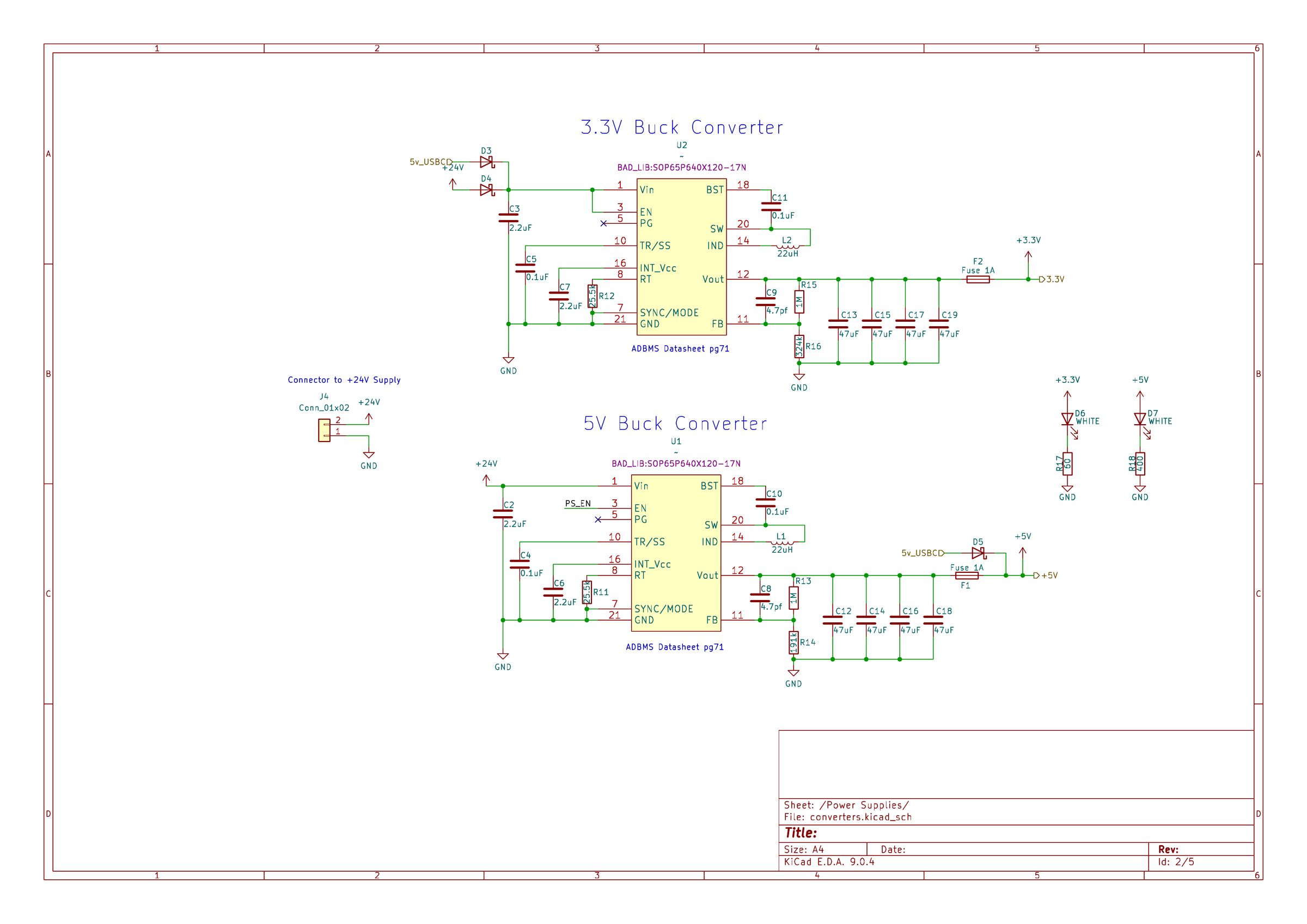
Both logic rails use TI LM5164DDA synchronous buck converters running directly from 24V (6–100V input range). Output voltage is set by a feedback resistor divider on each converter, and switching frequency is set independently by a single RT-pin resistor, keeping the two stages decoupled and individually tunable. Each rail has a 1A polyfuse and a white power-good LED for bench verification.
Charge Control Subsystem
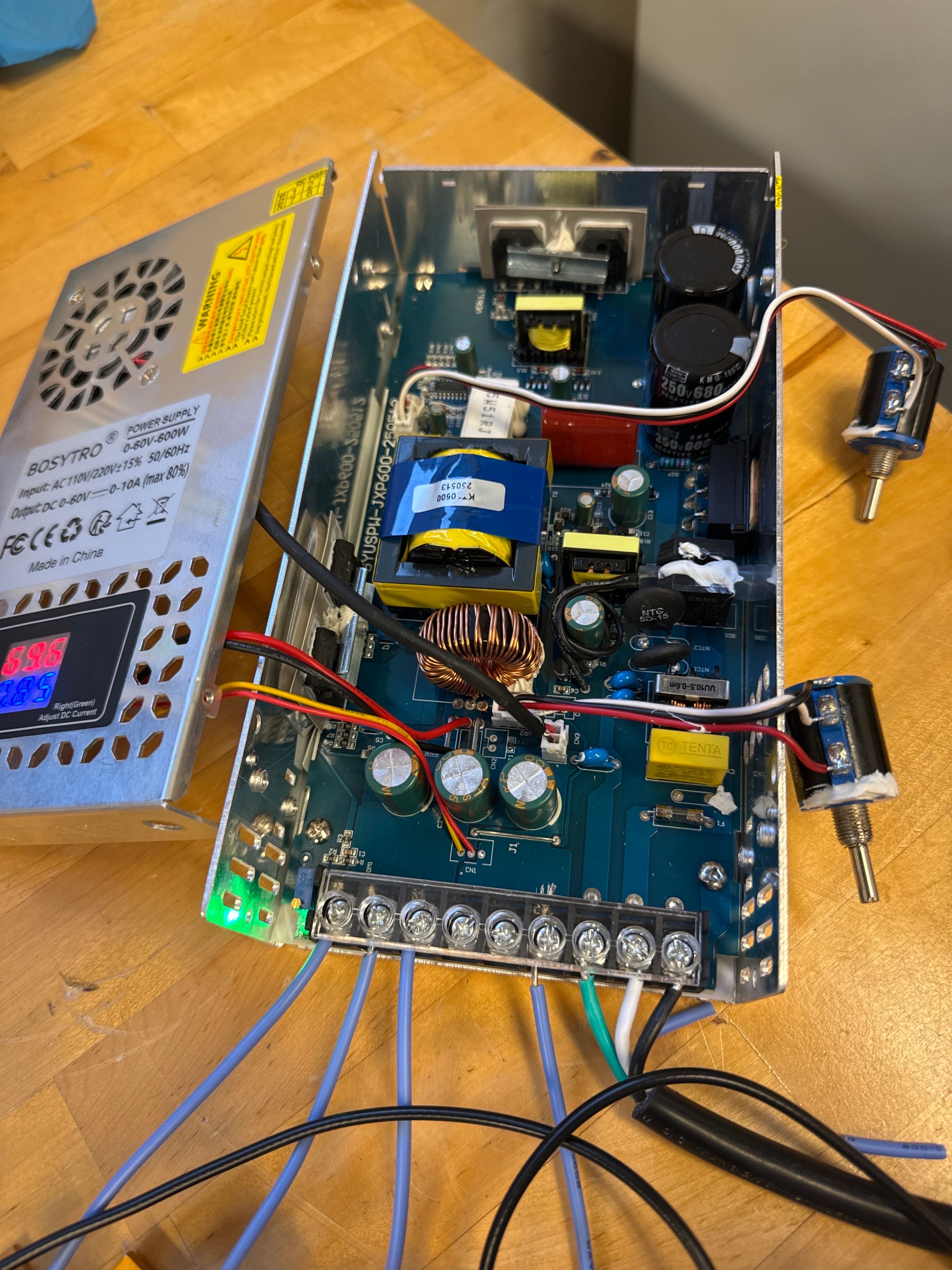
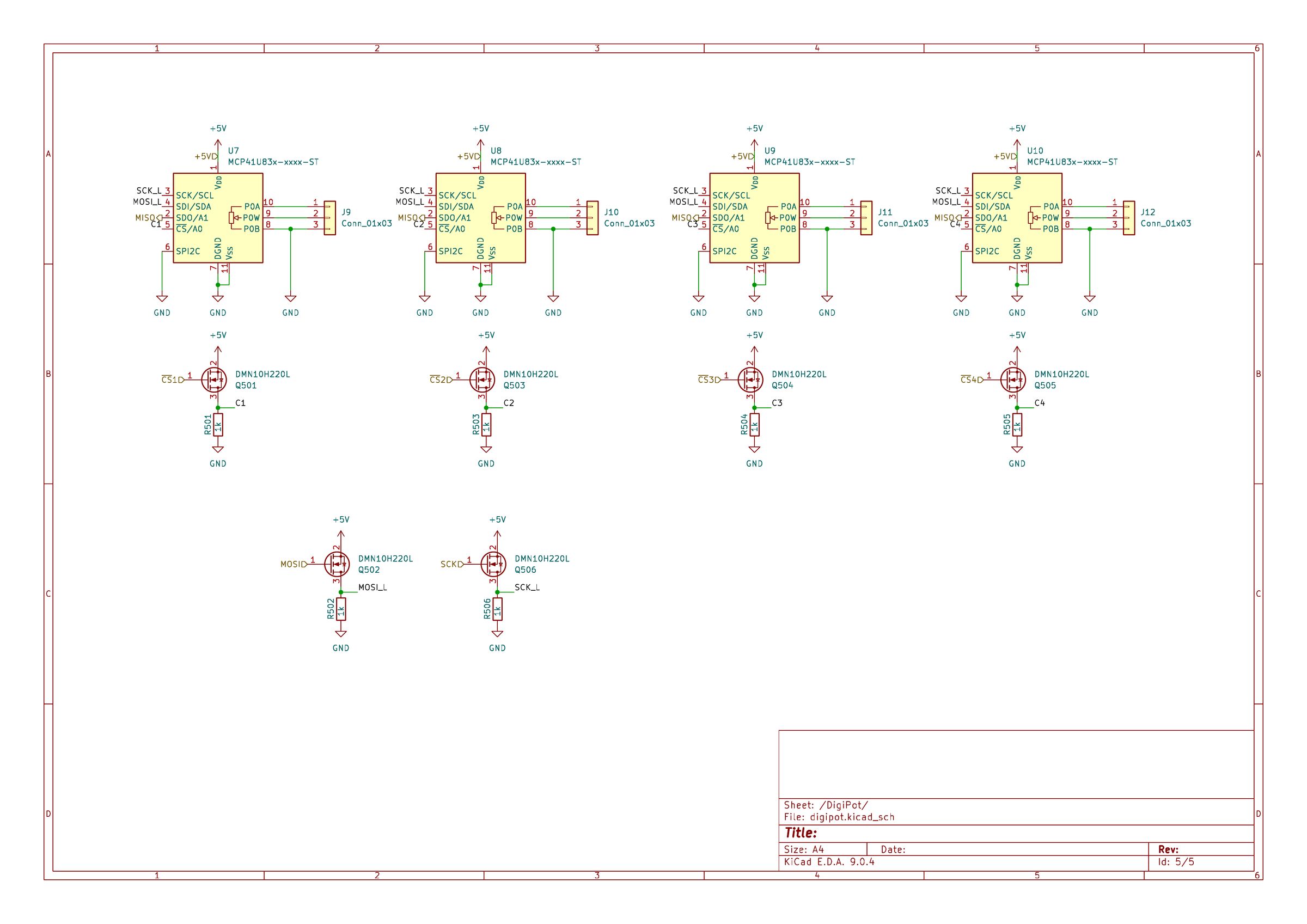
Industrial open-frame PSUs use a physical potentiometer to set their output voltage. Replacing that potentiometer with an MCP41U83T 10-bit SPI digital potentiometer gives the STM32 firmware control over PSU output voltage with no other modifications to the supply. Each DigiPot's P0A, P0W, and P0B pins connect directly to the corresponding terminals of the PSU's voltage-setting pot circuit. Incrementing the wiper position (0 to 1023 across a 5kΩ range) raises the PSU output voltage setpoint, allowing firmware to influence charge current while monitoring voltage and current feedback. Decrementing it reduces the voltage setpoint and tapers current.
All four DigiPots share SPI1 (PA5/PA6/PA7) with individual chip selects on PA8–PA11. The driver exposes MCP_Init(cs), MCP_Write(cs, value), and MCP_Read(cs), confirmed functional on all four channels.
The board is designed to support a CC/CV charging algorithm once the firmware state machine is complete. During the planned constant-current phase, firmware will adjust each PSU voltage setpoint to maintain target charge current based on current feedback. During the constant-voltage phase, firmware will regulate the PSU voltage setpoint near the pack target voltage while monitoring current taper toward the termination threshold.
Microcontroller and Peripherals
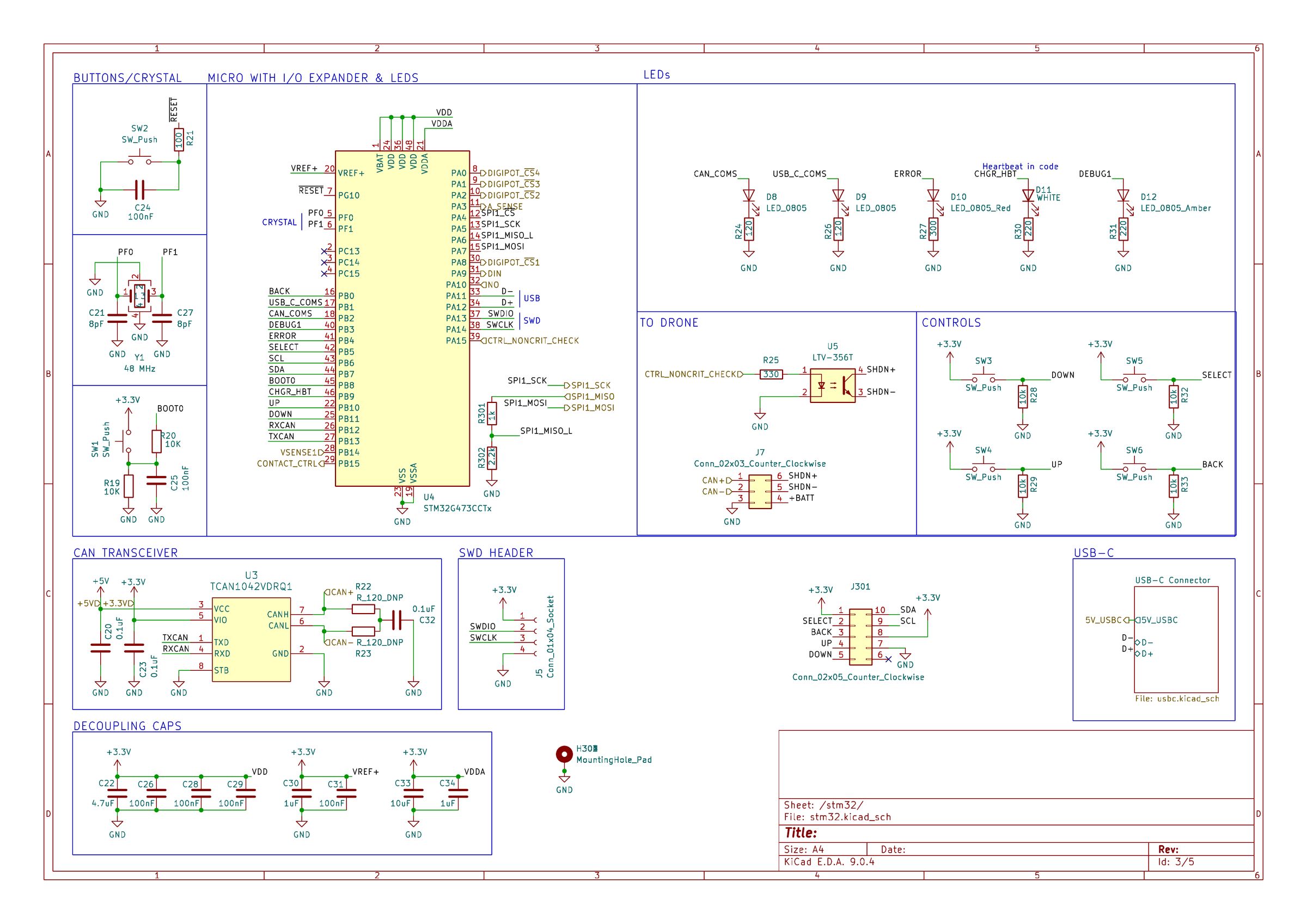
The STM32G473CCU6 (Cortex-M4 with FPU, 170 MHz, LQFP-48) was chosen for its native FDCAN peripheral, full-speed USB controller, hardware FPU for control-loop math, and sufficient SPI, I2C, and ADC resources in a 48-pin package.
Key peripheral assignments:
- SPI1 (PA5/PA6/PA7, CS PA8–PA11): Four MCP41U83 DigiPots
- FDCAN1: CAN-FD drone bus via TCAN1042VDRQ1 automotive transceiver (optional DNP termination)
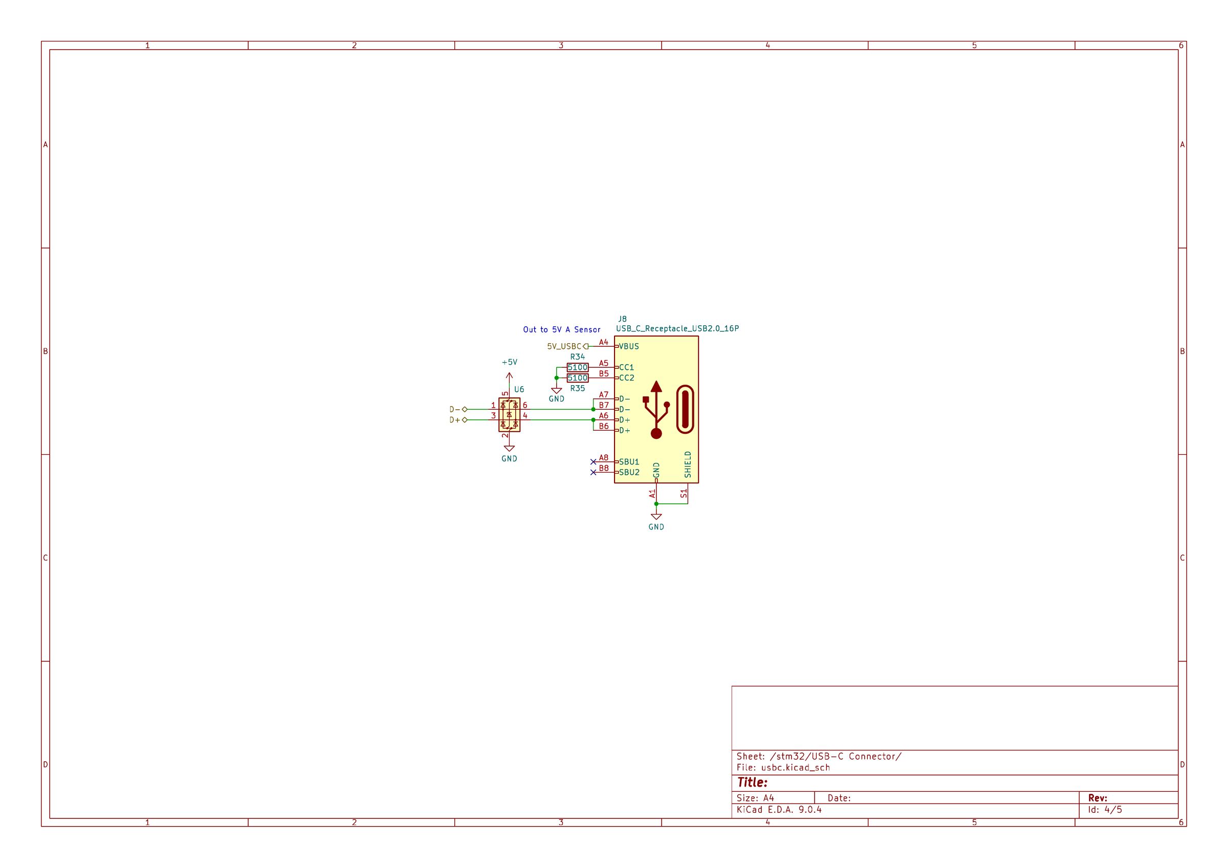
- USB FS: CDC virtual COM port via GCT USB4105-GF-A USB-C connector with USBLC6-2SC6 ESD protection
- I2C1: OLED display header
- ADC (PA3, per-channel inputs): Battery voltage via Schottky-clamped resistor divider; current via contactor sense signal
- GPIO PB15: Optoisolated high-power contactor driver (LTV-356T)
An external 48 MHz crystal provides a stable USB full-speed clock reference. The board also carries a 2x5 SWD debug header, six tactile buttons, five status LEDs, and an I2C OLED header.
Contactor and High-Power Switching
Each channel's PSU output (30–60V, up to ~120A) is gated by a high-power contactor before reaching the battery. The contactor serves two roles: it isolates the battery from the PSU when not charging, and it provides built-in current sensing that the STM32 reads via ADC.
The contactor coil is driven through an LTV-356T optocoupler between the STM32 GPIO (PB15) and the MOSFET that switches the coil supply. This isolates the 3.3V logic domain from the contactor coil drive voltage entirely. Battery voltage is sensed on the output side of the contactor through a Schottky-clamped resistor divider, giving the firmware visibility into actual battery voltage rather than PSU output voltage.
This isolation architecture reduces the likelihood of high-power-side faults propagating into the logic domain, and the contactor provides a hard electrical disconnect independently of firmware state.
PCB Layout
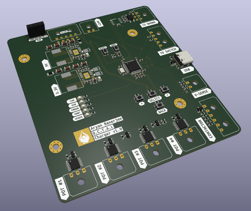
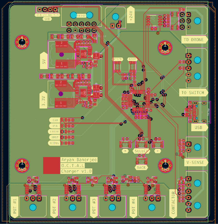
The board is zoned by function: buck converters on the left, four DigiPot channels along the bottom edge adjacent to the Molex Micro-Fit PSU signal connectors, STM32 centered, and all connectors on the perimeter. The board carries no charging current; the high-power path (PSU output to battery) is entirely external. SPI traces are kept short and routed away from the converter switching nodes.
Hardware Bring-Up and Debugging
The board has been fabricated and brought up on the bench. Three problems surfaced during bring-up, each traced to a specific root cause.
USB CDC Enumeration Failure
Problem: USB-C failed to enumerate after flashing initial firmware ("device not recognized").
Root cause: OCTAL_Set_Clock() switched the USB clock source to HSI48 after the USB peripheral was already initialized, leaving it with no valid clock.
Fix: Reorder initialization so the USB clock is active before the peripheral starts.
Result: USB enumerates reliably as a CDC virtual COM port.
Contactor Logic Inversion
Problem: Contactor_Set(CONTACTOR_CLOSED) opened the contactor instead of closing it.
Root cause: The LTV-356T optocoupler inverts the signal path. The initial enum values had the polarity backwards.
Fix: Corrected the enum definitions at the source rather than adding a per-call inversion.
Result: Semantically correct behavior throughout the entire codebase.
MCP_Read Returning 0xFF
Problem: MCP_Read() returned 0xFF on every call regardless of what had been written.
Root cause: The MCP41U83's SPI2C pin selects SPI or I2C mode. Left floating, the device does not drive SDO, holding MISO high. The firmware frame format was correct from the start.
Fix: Confirmed SPI2C tied to GND on the physical board, enabling SPI mode and activating SDO.
Result: MCP_Read() returns correct wiper values on all four channels.
Skills Demonstrated
- High-power system integration: Designed a control interface for four industrial PSUs (~24kW total), coordinating per-channel PSU voltage control, isolated contactor switching, and current/voltage sensing through a single embedded controller
- PCB design: Laid out a mixed-signal board in KiCad 9 covering switching power supplies, analog sensing, optoisolated high-power control, and multi-protocol digital communication
- Power electronics: Designed and sized two LM5164DDA synchronous buck converters from 24V, including feedback network, switching frequency selection, and per-rail polyfuse protection
- Embedded firmware: Brought up SPI, ADC, USB CDC, and GPIO on STM32G473; wrote a four-channel SPI driver for DigiPot-based PSU voltage control per channel
- Hardware debugging: Diagnosed USB clock ordering failure, optocoupler signal inversion, and DigiPot SPI/I2C mode pin misconfiguration on the fabricated board, each isolated to root cause using SWD and ST-Link
- System design: Designed optocoupler isolation for high-current contactor control, multi-device SPI with per-channel chip selects, and separation of the 24V logic domain from the 30–60V charging path
Status and Next Steps
Validated on hardware:
- 5V and 3.3V rails stable
- STM32G473 programs and runs via SWD
- USB-C enumerates as a CDC virtual COM port
- Contactor opens and closes correctly under firmware control
- Per-channel voltage and current sensing via ADC confirmed
- SPI DigiPot driver functional on all four channels
Planned for next milestone:
- CC/CV charging finite state machine for all four channels
- CAN-FD driver and drone BMS message protocol
- Button debounce, LED state machine, and OLED I2C display driver